7805 REGULATOR Schematic
Recent Post
RANGKAIAN 7805 REGULATOR
7805 REGULATOR Schematic
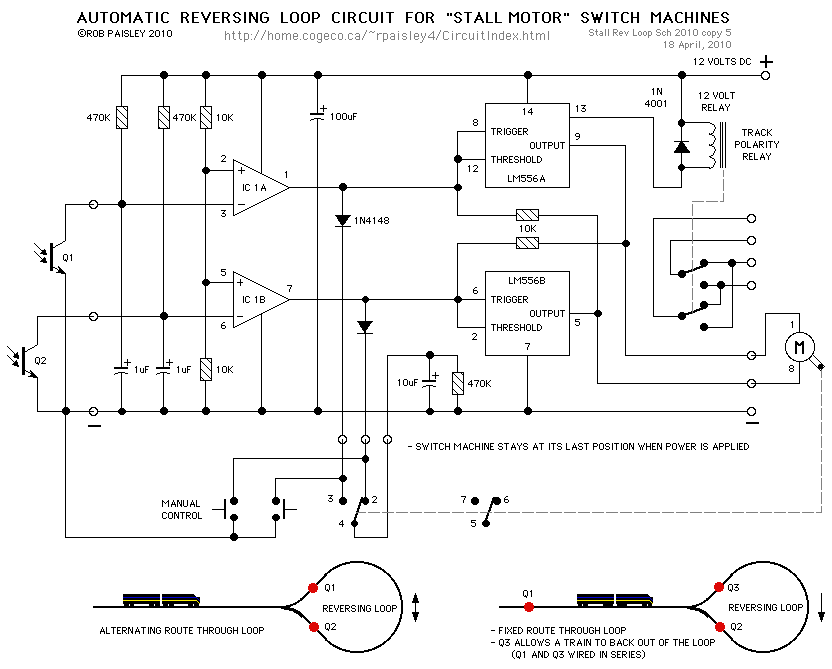
Loop Control Automatic Reversing Circuit
*
It is not the purpose of this page to provide a detailed explanation of the IC's used by this circuit. If you want more information on this subject please refer to the Flip-Flop Made With A LM556 Timer Chip page in the miscellaneous circuits section of this site and also the Visible Light Photo Detector Circuits.
*
The circuit uses the basic phototransistor detector circuit to sense the position of a train that is approaching or is in the reversing loop.
*
Track polarity reversing is not covered by this page and will have to be determined by the user.
Please Read Before Using These Circuit Ideas
The explanations for the circuits on these pages cannot hope to cover every situation on every layout. For this reason be prepared to do some experimenting to get the results you want. This is especially true of circuits such as the "Across Track Infrared Detection" circuits and any other circuit that relies on other than direct electronic inputs, such as switches.
If you use any of these circuit ideas, ask your parts supplier for a copy of the manufacturers data sheets for any components that you have not used before. These sheets contain a wealth of data and circuit design information that no electronic or print article could approach and will save time and perhaps damage to the components themselves. These data sheets can often be found on the web site of the device manufacturers.
Although the circuits are functional the pages are not meant to be full descriptions of each circuit but rather as guides for adapting them for use by others. If you have any questions or comments please send them to the email address on the Circuit Index page.
LM56 Thermostat Project Circuit Diagram

LM56 Thermostat Project Circuit Diagram values of R1, R2 and R3 for the required trip points VT1 and VT2 can be determined using the subsequent equations.
VT1 = 1.250V x (R1)/ (R1 + R2 + R3)
VT2 = 1.250V x (R1 + R2)/ (R1 + R2 + R3)
where:
(R1 + R2 + R3) = 27 k Ohms and
VT1 or T2 = [6.20 mV/degree Celsius x T] = 395 mV therefore:
R1 = VT1/ (1.25V) x 27 k Ohms
R2 = (VT2/ (1.25V) x 27 k Ohms) – R1
R3 = 27 k Ohms – R1 – R2
Rangkaian USB Sound Card PCM2702
PCM2702 needs only few additional parts to work. The schematic is not complex. Sound card can be powered directly from USB port (jumper W1) or from external power supply (jumper W3). PCM2702 needs two power supply 3.3V (3V-3.6V) and 5V (4.5V-5.5V). I used fixed output voltage LDO TPS76733Q for 3.3V (IO2) and adjustable output voltage LDO TPS76701Q for 5V (IO3). Both LDO are produced by TI, I used this because I had it in my drawer. Any similar LDO can be used. Output voltage of IO3 should be set to little bit lower than input voltage to allow LDO good stabilization, in my case output voltage is set to 4.8V. Output voltage can be set by adjustable resistor R33. In case of low power supply, IO3 can be shorted by jumper W3. LED D3 signalizes power on.
Small ferrite beads are placed before all power pins of PCM2702 and in Vbus and GND of USB. These small beads reduce high frequency hum. I had a problem find this small SMD ferrite beads in local stores but finally I acquire few of them from old hard drive. They are not absolutely necessary, you can use zero ohm resistors instead of them.
Low-pass filter is placed in output signal path to reduce sampling frequency. An OPA2353UA dual op amp is configured as a stereo 2nd-order low-pass filter. Led diode D1 is illuminated when PCM2702 plays audio data received from the USB bus. Led diode D2 is illuminated when USB bus suspends audio data transmission to the PCM2702.
Rangkaian Infrared Cordless Headphone Amplifier

Rangkaian Op-amp Headphone Amplifier RC-4560
View More here...
Tube Preamplifier Schematic 6DJ8 / ECC88 SRPP
This is one of many possible variations for a Symmetrical SRPP Preamplifier based around the 6DJ8 / ECC88 family of tubes. The SRPP circuit has also been referred to as a SEPP, Totem Pole, Mu Follower, Mu amplifier and Cascoded Cathode Follower. The original name for this circuit is a Balanced Direct and Alternating Current Amplifier (Maurice Artzt, Radio Corporation of America, February 9, 1943, Patent 2310342).

6DJ8 / ECC88 SRPP Tube Preamplifier Schematic
Tube Preamplifier 5687 Led Biased Circuit


Rangkaian MOSFET Hybrid Headphone Amplifier 12AU7 / IRF612

Table 1: Parts List - 12AU7 / IRF612 Headphone Amp
| QTY | LABEL | VALUE |
|---|---|---|
| 2 2 2 2 2 2 2 2 2 2 2 1 2 1 1 1 | P1 C1 C5 R1 C2 R5 R4 R3 C4 R2 R6 VT1 T1 -- -- -- | 100k 100nF 100nF 1M 1uF 20ohm 5W 200 ohm 2W 220k 2W 470uF 50V 47k 5k 2W 12AU7 / ECC82 IRF612 LED Holder LED 9-pin Tube Socket |
Additional Notes - Parts List:
Rangkaian Audio Amplifier 25 Watt Mosfet

Parts:
Kit
R1,R4_________47K 1/4W Resistors
R2____________4K7 1/4W Resistor
R3____________1K5 1/4W Resistor
R5__________390R 1/4W Resistor
R6__________470R 1/4W Resistor
R7___________33K 1/4W Resistor
R8__________150K 1/4W Resistor
R9___________15K 1/4W Resistor
R10__________27R 1/4W Resistor
R11_________500R 1/2W Trimmer Cermet
R12,R13,R16__10R 1/4W Resistors
R14,R15_____220R 1/4W Resistors
R17___________8R2 2W Resistor
R18____________R22 4W Resistor (wirewound)
C1___________470nF 63V Polyester Capacitor
C2___________330pF 63V Polystyrene Capacitor
C3,C5________470µF 63V Electrolytic Capacitors
C4,C6,C8,C11_100nF 63V Polyester Capacitors
C7___________100µF 25V Electrolytic Capacitor
C9____________10pF 63V Polystyrene Capacitor
C10____________1µF 63V Polyester Capacitor
Q1-Q5______BC560C 45V 100mA Low noise High gain PNP Transistors
Q6_________BD140 80V 1.5A PNP Transistor
Q7_________BD139 80V 1.5A NPN Transistor
Q8_________IRF530 100V 14A N-Channel Hexfet Transistor
Q9_________IRF9530 100V 12A P-Channel Hexfet Transistor
Parts:
R1____________3K3 1/2W Resistor
C1___________10nF 1000V Polyester Capacitor
C2,C3______4700µF 50V Electrolytic Capacitors
C4,C5_______100nF 63V Polyester Capacitors
D1__________200V 8A Diode bridge
D2__________5mm. Red LED
F1,F2_______3.15A Fuses with sockets
T1__________220V Primary, 25 + 25V Secondary 120VA Mains transformer
PL1_________Male Mains plug
SW1_________SPST Mains switch
Notes:
* Can be directly connected to CD players, tuners and tape recorders. Simply add a 10K Log potentiometer (dual gang for stereo) and a switch to cope with the various sources you need.
* Q6 & Q7 must have a small U-shaped heatsink.
* Q8 & Q9 must be mounted on heatsink.
* Adjust R11 to set quiescent current at 100mA (best measured with an Avo-meter connected in series to Q8 Drain) with no input signal.
* A correct grounding is very important to eliminate hum and ground loops. Connect to the same point the ground sides of R1, R4, R9, C3 to C8. Connect C11 to output ground. Then connect separately the input and output grounds to power supply ground.
* An earlier prototype of this amplifier was recently inspected and tested again after 15 years of use.
Rangkaian SMS Remote Controller V3.0

Picture 1: The SMS remote controller V3.0.
Introduction.
It's been passed a lot of years since my first SMS remote control. The reason I stoped developing the source code of my previous circuit was that the T10s was not available in the market sinse a lot of years. So, people could not find very easy that cell phone to build the circuit. Two years later I built another one remote control based on GSM module. I choose the GM-47 sony-ericsson module because it was very easy to handle it via AT commands. Moreover, the price was low enough for experiments. Finaly, I decided to release the source code under GNU General Public Licence V3 If you don't agree with the terms please DO NOT download or use any part of this project (schematic diagram, source code, hex code, PCB, etc).
What is this circuit for?
With this circuit you can power-ON or Power-OFF a lot of electric/electronic devices such as aDSL modem, personal computers, water boilers, water pumps, garage doors, lights and many more. Moreover, you can watch the status of 8 switches. These switches can be connected with reed switches to the windows and the doors of your house. Just like a security system.
The circuit I have made has the following specifications:
| - 4 relays to Power-ON or OFF any electronic/electric device. - 8 digital inputs for reading normal swiches or reed switches. - Very few and cheap components. - SMS command execution is protected under a programmable password (for avoiding false SMS commands from other persons). |
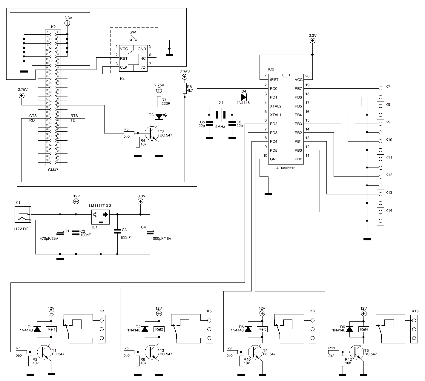
Picture 2: The schematic diagram of SMS remote control v3.0 (click to enlarge).
The schematic diagram.
This circuit is constituted by an AVR micro-controller (ATtiny2313) at 4MHz, the GM-47 GSM module, a SIM card and 4 relays. The GM-47 module works at 3.3V and is powered by the voltage stabilizer IC1. The micro-controller IC2 can work with power from 2.7V-5.5V when the speed is under 10MHz. So we power it at 3.3V because this is the voltage level that works GM-47 module. The data connection between GM-47 and ATtiny2313 is done at 9600 bps. The voltage level for this comunication is 3.3V from AVR's side and 2.7V from GM-47 side. Because of this voltage difference I used the T5 transistor to do the voltage level adaptation.
The connection of the SIM card with the GM-47 is been made by the SIM-holder K15 and the presence of the SIM card into the SIM-holder is been made by the swich SW on SIM-holder. The LED D6 when it flases, indicates that the connection to the cell phone network has been done properly. When the module cannot been connected to any cell phone network, the LED stays always ON (it's not blinking).
The GM-47 has digital and analog inputs-outputs it self but I didn't use them to avoid a malfunction with the danger of destroying the GSM module.
What the AVR micro-controller does.
After you power-on the circuit the IC2 (ATtiny2313) waits until GM-47 is initiallized, by reading the SIM card and connects to the GSM network that SIM card supports. After the connection to the network, the AVR sends the command
If there is an SMS, the AVR reads it and checks if there is the correct password. Initially the password is 1234 and can be changed by the user. Then, checks if the next character is the "*" (star). This symbol means: "Change the password with the following 4 numbers or letters". Then is searching to find the words
At the end the AVR deletes the SMS from the GM-47 first storage address and starts over sending again the AT commands .
Sending an SMS to the remote control
You can send an SMS from any cell phone to the remote control by following one of the above command syntax:
| A) 1234*5678 Relay1=1 Relay2=0 Relay3=1 Relay4=1 Status B) 1234 Relay1=1 Relay2=0 Relay3=1 Relay4=1 Status C) 1234 1=1 2=0 3=1 4=1 Status D) 1234 Status E) 1234 Relay2=0 |
In case A we have the maximum of selections. We send the initial password 1234 and we change it to 5678. We arm the relay-1, relay-3, relay-4 and disarm the relay-2. Moreover, by writing the word
In case B we arm the relay-1, relay-3, relay-4, disarm the relay 2 and ask for the status of the relays and the switches.
In case C we do the same bypassing the words
In case D we ask only for the status of relays and switches.
In case E we change the status of only one relay. In this case relay-2 will be disarmed.
|
Piucture 5: The placement of the GM-47 module on the PCB. See the yellow thin film I put under the connector. This film is been put to protect the circuit from shortcuts between copper strip and the connector. |
Rangkaian FM Wireless HI-FI
To relieve you of any concern related to high frequency, I used a module ready, in case a module Aurel audio FM transmitter. This tiny circuit board with 2 cm by 4 cm supports a transmitter modulation frequency track, delivering an RF power of 10 mW which is quite sufficient for the desired use. As it is driven by a resonator surface wave, its frequency stability is excellent.
As you can see the review of the scheme, the module can stand alone even for some HF itself since it lacks power and a network of pre-emphasis R7, R8, C6, designed to improve quality transmission of higher frequencies.

The input level required by the circuit to achieve a sufficient modulation rate of 100 mV rms, a preamplifier is necessary for our microphone. It is the role of IC1, mounted on a very classic inverting amplifier with adjustable gain through P1.
The provided microphone is a model electret with its supply circuit formed by R1, R2 and C1, but you might as well use a conventional dynamic mic, or an external electret microphone with its integrated power supply in which case R1, R2 and C1 disappear.
2. Receiver
As illustrated, the audio output takes place on the leg 10 of the module and should be désaccentuée through capacitor C4 to offset the effect of pre-emphasis circuit used in the show. The AF level issued by the module may be insufficient for some high fidelity amplifiers or mixers certain: it is only 100 mV in the best cases I amplifies a bit through rose IC1 very classic.

In order not to saturate the amplifier or mixer that follows, the adjustable potentiometer P1 can measure the level applied to it.
This preamplifier is fed continuously as the module Aurel but instead receives its power through the leg 18 of the latter. This output is in fact controlled by the internal circuit noise and is connected to power when the circuit noise estimates have detected a valid issue. The operating threshold of the muffler is adjustable and is obviously the role of the potentiometer P2 is the only external control of the receiver.
The food in turn must be regulated to 5 volts, which is made by IC2 which can receive input from 9 to 15 volts from such amplifier associated with a block or sector-style outlet . The low power consumption of the arrangement (of the order of 30 mA) makes this power supply.
MIC 640 Acquisition System Analog Versatile Circuit
This tour, available in Stainless DIL 8 legs, can measure 4 analog voltage independent between 0 and 5 volts, and send the result of this measure in the form of four characters on a standard asynchronous serial link. Its serial output is directly TTL or CMOS compatible and can be connected to a serial input RS 232 by simply adding a resistor.
The MIC 640 can operate in automatic mode, thus sending the result of four steps every second, or in command mode, in which case it sends the result of four measures under the control of external logic signal. In this latter method that we use here.
Its consumption is extremely low, it is possible to feed signals from the unused serial port RS 232, subject of course not to waste the little energy available in external circuits involved too greedy.
This circuit, easily available in France, costs less than 18 euro which makes it an ideal candidate for this achievement we will find the schema without tarder.Si you want more information about the MIC 640;'s complete data sheet entirely in French, is available for download by clicking this link.
Schematic acquisition module

The heart of the module is obviously the MIC 640, spotted IC1 on the figure below. It is directly connected to the serial input RS 232 PC via limiting resistor R1 current.
His entry called CTRL to define its mode of operation. Left to the body, it makes it automatically perform a conversion on each input per second, whereas if it is reduced to levels as high as in this case, it triggers a conversion of each entry at each grounding.
These earthed take place through the transistor Q1 controlled by the serial data output TXD of RS 232, via the diode D4. This same output is through the diode D3 and this time the capacitor C3, to produce the negative supply voltage of the input stage that we discover in a moment.
The control lines DTR and RTS serial interface they provide for the positive supply via diodes D1 and D2. This voltage is unregulated, is the positive power of the input stage. By cons, it is regulated to 5 volts through IC2 so that it feeds a voltage very stable MIC 640.
As the current and available for both the positive supply for the negative supply is still low (10 mA max), I had to carefully choose the components used and they will not be replaced under any pretext. IC2 is indeed a regulator 5 volts 3 feet very low: in one case in 2936 SM Z5 which absorbs only 500 uA. For information, its "equivalent" the 78L05 consumes 3 mA in the same situation!
The input stage meanwhile was achieved using four operational amplifiers effect transistor field-mounted voltage followers. This confers to the module input impedance greater than 100 MW. All four amplifiers are combined in one box, referenced LF 444 at National Semiconductor, whose total consumption does not exceed 800 uA for the four amplifiers! Again, no question of putting such a TL 084 which face voracious with its 5.6 mA!
This input stage is protected from excessive voltages through resistors R7 to R10 and diodes D6 to D13. If you precede the various stages of converting physical quantities / voltage, you can possibly do without protection diodes that degrade somewhat the very high input impedance of 444 MQ due to their leakage current. It is in fact only 50 pA maximum input of 444 LF while a diode, even small leaks, easily misses 1 nA or 20 times more!
PIC Universal Programmer Schematic

This can only supply circuit to program only when really necessary and thus avoid any problems during its insertion or extraction of its programming support. Two red LEDs, D1 and D2 indicate the presence of tension on the support. D3 for its light just when the timer is turned to signal the proper functioning of the food.
Data to be programmed by IC1A pass while they go through IC1b at a replay of the circuit. The clock programming through IC1c. Support for receiving circuits to program is a model 40 feet a bit special so they can receive the PIC cases: 8, 18, 20, 28 and 40 feet. The wiring of different supplies, the data line and clock line is made in accordance with the pinouts of the various circuits.
The feeding program is simple but very tolerant. Two stabilized voltages are required: 5 volts to 13 volts and VDD for programming voltage VPP. IC2 is a 78L05 loads of 5 volts while IC3, which is a 78L08, produces 13 volts because it is not referenced to ground but the output of IC2 and product and 5 + 8 or 13 volts! To accept any external source, regulators are preceded by a generous filter and bridge rectifier. You can apply any J1 AC voltage between 12 volts and 20 or between 16 and 30 volts. The flow required is only about 100 mA.
Figure Programmer Circuit Of AVR Atmel Microcontroller
The scheme of my program boils down to what you can find below. It is intended to be connected to the PC parallel port lines which are easy to fly by the program to generate the necessary timing.
It comprises all in all an integrated circuit IC1, which is a simple 74HC244 or 74HCT244, that is still a buffer for six times to reformat the signals transmitted on the PC printer output before applying the circuit to program in April. It is safe and to have a rectangular shape and signals to avoid any hazard of programming.
This circuit is wired to "amplify" signals SCK, MOSI and RESET the one hand, since these are the PC to the microcontroller, and the only signal MISO, in another sense, since it will the microcontroller to the PC.
Note that a section of IC1 LED driver from the PC which allows to report, by the ignition, the microcontroller is being programmed and it must not touch it! Power to the programmer is supplied directly to the application supporting the microcontroller via the diode D1.
MIC 702 Mictronics Schematic Diagram
Sms Remote Control For Sony Ericsson T10

The firmware of the AT90S2313 (or ATtiny2313) its actual complicated because, we accept to catechumen the 'septets' of the buzz to 'octets' because the AVR charge bytes with 8 $.25 breadth ( The 'septet' is 1 byte with 7 $.25 breadth and 'octet' is 1 byte with 8 $.25 length). All this proccess its all-important to break the bulletin from SMS.
This ambit is alive on both AT90S2313 and ATtiny2313 microcontrollers. In case of ATtiny2313 you accept to baddest "External Crystal Oscillator" instead of absence "internal RC oscillator" from the "Fuses" tab of your programmer's software. You accept to uncheck the "Divide alarm by 8 internally".
When you accomplishment the ambit affix it to the adaptable phone, about-face on the buzz and afresh ability on the circuit, not afore . The AVR now its aggravating to apprehend the bulletin from the 1st anamnesis area of the phone, for that i advance to annul all SMS letters from the buzz afore affix it to the circuit. If there is no bulletin to the 1st anamnesis location, the AVR its aggravating afresh until you beatific any.
The architecture of the bulletin charge be abandoned '1' or '0'. '1' to enable, or '0' to attenuate the device. The bulletin charge accept abandoned 8 numbers, '1' or '0' , abandoned or alloyed .
Example: if you accelerate the bulletin 11000100 afresh you enable, starting from the right, the accessories 3,7,8 ('1') and disabling the accessories 1,2,4,5,6 ('0') .
If you appetite to accelerate a new bulletin and you don't appetite to change some device, charge accelerate the aforementioned cardinal as the old message.
Example: If you appetite to accredit abandoned the 5th device, you charge accelerate a new bulletin like 11010100 to accumulate the added accessories as there are (we accelerate the aforementioned bulletin as the old ( 11000100 ) and we change abandoned the 5th bit from '0' to '1' to accredit the accessory ).
RF Remote Control 2 Channel

The RLP434A is an RF receiver bore with cancellation abundance at 418MHz with ASK modulation. There are 2 outputs from this module, the digital, with levels from 0v to VCC (5 volts in our case) and the analog output. Analog achievement is not used. The transmitter accelerate 4 bytes with 2400bps 4 times and the receiver RLP-434A, aggregate them and move them to AT90S2313 to RxD pin, PD0.
Two affidavit to baddest AT90S2313 (20pins) instead of AT90S2343 (8pins) is because
a.) AT90S2313 use a accouterments UART adapted at 2400bps and the accouterments UART is added stable, with abate code, than software UART that I use in the transmitter. If some consecutive abstracts access at the middle-time of some added accepted added than accept routine, for abiding we will apart this $.25 of data. The accouterments UART does not accept this botheration because accept absorber for this (UDR register). This is what I beggarly that the accouterments UART is "stable".
b.) with AT90S2313 we can drive up to 14 relays with approaching advancement of the firmware, one broadcast to anniversary pin.
As antenna you can use a cable 30 - 35cm long

* The array abridgement is fabricated it by the use of powerdown approach of AVR. In this case the AVR goes to beddy-bye with beneath than 1uA (microampere) accepted and delay for alien arrest on pin PB1 to alive from beddy-bye and abide operating.
If you columnist the S2 key, the argumentation of this pin goes to '0' (0V) and AVR alive frome the beddy-bye approach (because PB1 is INT0) and analysis if apprenticed the S1 key. If not, the AVR booty as apprenticed key the S2. If yes the AVR booty as apprenticed key the S1.
If you columnist the S1 key the argumentation of this pin and PB1 (through 1N4148) goes to '0' (0V). In this case the AVR booty as apprenticed key the S1.
After, account the checksum and address 4 times the aforementioned 4 byte arrangement to accomplish abiding that receiver takes the abstracts and goes to beddy-bye approach until abutting arrest on PB1.
When the INT0 pin (PB1) of AVR goes to 0V, the transmitter TLP434A is working. If you stop columnist the about-face S1 or S2, the TLP is stop working.
* The safe transmition of the abstracts based to transmition of 4 bytes with consecutive anatomy at 2400 bps (bits per seconds). 1st and 2nd byte are for acceptance of accurate alien ascendancy from receiver (like ID bytes), 3rd byte is command byte. The relays cachet dependet by the amount of this byte. Finaly, the 4th byte is the checksum of the beforehand 3 bytes.
example: if byte1=30h, byte2=35h and byte3=02h the 4th byte (chechsum) will be (byte1) XOR (byte2) XOR (byte3) = 30h XOR 35h XOR 03h = 06h.
This adjustment use 4 bytes x 8 bit anniversary = 32 bit breadth (without alpha and stop bits). That is beggarly 1 achievability at 4.294.967.295 to accept the receiver, the aforementioned 4 bytes from some added RF device.
This transmitter will assignment with all 2323 chips but bigger is AT90LS2323 with alive voltage 2.7 - 6 volts.The microcontroller that I use is AT90S2323 with alive voltage 4 - 6 volts. Its formed accomplished with 3v lithium battery.
As antenna you can use ~7cm cable in to transmitter`s box.
PAL Colour Bar Generator With AT90S2313

The aboriginal abstraction was to assignment with 8.867238 MHz clear (2 times the blush carrier). When I apprehend added about PAL video blended arresting creation, I saw that if you appetite to artefact colors entire-in-software you charge actualize the color-carrier (4.43 MHz), alteration 4 times the appearance of color-carrier (one time for anniversary color), to appearance 4 colours. Except that, you accept to change the color-burst from 135 deg to 135+90= 225 deg.
So, the 8.86 MHz is not enough, that`s why I acclimated 17.7 MHz clear (4 times the blush carrier). The accessible affair is to actualize the white and the atramentous bar, the blow of this project, beleave me, it's not easy.
The timing (clock cycles) of any apprenticeship is actual important for the phase-shift of the color-carrier and color-burst signals. You should account the cycles afore add or abolish any instruction.
The circuit
The ambit iis constituted by AT90s2313 active at 17.734475 MHz (overclocked) and a , 5-bit DA advocate (R2R-ladder) with 10 resistors.
I know, it's not a acceptable abstraction to overclock 77 % high than the alive abundance of the MCU, but for a few hours, annihilation amiss will happen.
Programm (write) the MCU with colour_bar_gen.hex that it's included in colour_bar_gen.zip file, affix it on blended video adapter (or scart adapter) of your TV, power-on the ambit and you will see on TV, 6 vertical bars, 4 in color, 1 white and 1 black.
I won't accomplish any account about "how does the PAL video arresting is working" because I will charge a lot of web pages to do that. Maybe some one of you, accept the ability and the time, to abide this project..
via
OpAmp Voltage Indicator Using LM741 Circuit
The LM741 specification sheet can be downloaded here.