Recent Post

OpAmp Voltage Indicator Using LM741 Circuit

LM741 Low Voltage IndicatorLM741 Low Voltage Indicator Circuit

In order to obtain a low voltage indication - useful if you would like to stop using a battery before it is drained too deeply - the output from pin 6 is still directed through an LED (and current limiting resitor), but this time it is connected to ground rather than to the input voltage Vin as shown in the amended circuit diagram above.

Note that this circuit will only operate with input voltages in excess of around 3.8 Volts and so it cannot be used with a 2 AA battery charger.

LM741 High Voltage IndicatorLM741 High Voltage Indicator

The circuit diagram shown above is configured to give a high voltage indication. The 100KOhm variable resistor is used to manually configure the voltage over and above which the LED will light. If the voltage arriving at pin 2 of the LM741 is greater than the voltage arriving at pin 3, the LED lights thanks to the output from pin 6. At all other times the LED is off (as is the output from pin 6).

The Zener diode should be chosen with a zener voltage of around half that of the target voltage - e.g. for a 12.0 Volt indicator, a 5.6 Volt Zener diode could be used.

The LM741 specification sheet can be downloaded here.
Read MoreOpAmp Voltage Indicator Using LM741 Circuit

Light Dark Sensor With Relay Circuit Using LM741

Light Dark Sensor With Relay Circuit Using LM741
Above is a schematic diagram of an LM741 light/dark sensor circuit (from the excellent 741 Op-Amp Tutorial by Tony van Roon).
The ECG128/NTE128 transistor stipulated can be substituted with any NPN transistor rated at sufficient gain and current for the chosen relay coil.

1st Nov 2007 Update - We have modified the schematic diagram above with the addition of a 220uF smoothing capacitor between the base of transistor Q1 and ground. Without this capacitor, the relay chatter (relay switching on and off many times per second) was terrible around the switch on/off light level. By adding the capacitor, relay chatter was completely eliminated.

According to the designer of this circuit, the relay will be closed only when "NO light falls on LDR1", however, in testing this circuit proved to work very well with the user able to adjust the potentiometer (P1) to automatically close the relay at whatever light level they chose.

By swapping the postitions of the 10K resistor (R1) and the LDR (LDR1), the relay will be closed when the LDR is under light rather than under darkness. Therefore a device can automatically be switched off at nighttime.

Since this circuit still contains a relay we need to make some changes* to reduce the amount of power to make it more suitable for renewable energy powered low-current applications.
Read MoreLight Dark Sensor With Relay Circuit Using LM741

Skema Rangkaian Timer Menggunakan IC 4060B

Skema Rangkaian Timer Menggunakan IC 4060B

There are many applications for which a timer is very useful to turn a device on or off automatically after a preset interval - for example, switching off an irrigation system after 30 minutes of use, turning off a battery charger to prevent overcharging, etc.

Timing short intervals of milliseconds to minutes can easily be achieved using a NE555 timer chip. Unfortunately, this device is not suitable for timing longer intervals, and so a suitable alternative is required.

A schematic of the 4060B chip is provided below:


The pins labelled in red Q4-Q14 are the binary outputs: Q4 for the 16's, Q5 for the 32's, Q6 for the 64's and so on up to Q13 for the 8192's, and Q14 for the 16384's.

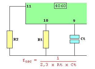
Just three external components are required to control the 4060B counter - two resistors and one capactor. The frequency of the internal oscillator (i.e. the speed of the count) is set according to the equation given at the bottom of the schematic below:


Since Q14 represents the 16,384's and Q4 represents the 16's - we know it will take 1,024 times longer (16,384 / 16) for Q14 to flip from 0 to 1 than it takes Q4. So, for an example 2-hour timer (=7,200 seconds), we just need to fine-tune the circuit so that Q4 turns on after 7,200 / 1,024 seconds = 7.03 seconds, knowing that if that is done correctly, after exactly 2 hours Q14 will flip from 0 to 1.
Read MoreSkema Rangkaian Timer Menggunakan IC 4060B

Nestbox Solar Powered Wireless CCTV Camera Circuit

Below is the circuit used to power the CCTV camera, provide lighting inside the nestbox, and charge batteries from a PV solar panel.
Circuit diagram for CCTV powered by Solar Panel with Battery Backup


D1 is a Schottky Diode used to prevent battery charge escaping through the solar panel at night. Something like a 1N5817 (1 Amp 20 Volt diode) will do the job and it has a very low voltage drop of under 0.45 Volts. D2 and D3 are ultrabright LEDs used to illuminate the inside of the nestbox. R3 and R4 are resistors chosen (400+ Ohms) to ensure that no more than 30mA of current gets to the sensitive LEDs, with R5 (a 10k variable resistor) used to increase the resistance and therefore dim the LED s if they are too bright.The LM317T is a voltage regulator * used to bring the voltage of the solar panel and batteries down to just over 8 volts using resistors R1 (270 Ohm) and R2 (1500 Ohm) to set this value. K is the wireless CCTV camera. A switch (not labelled) is used to manually turn the camera on and off as required.

Via : reuk.co.uk
Read MoreNestbox Solar Powered Wireless CCTV Camera Circuit

SPI Flash Programmer Circuit Diagram

SPI Flash Programmer Circuit DiagramSPI Flash Programmer Circuit Diagram

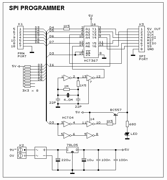
The Picture beneath is shows the ambit diagram of the SPI Flash programmer accouterments interface, the ability to the interface is provided either by a 9V dc adapter or a 9V battery. The 74HCT367 IC absorber the alongside anchorage signals. It is all-important to use the HCT blazon IC in adjustment to accomplish abiding the programmer should additionally assignment with the 3V blazon alongside port. The 74HCT04 is acclimated to accomplish the alarm arresting for the u-controller back programming the accessory in stand-alone mode.
Read MoreSPI Flash Programmer Circuit Diagram

Rangkaian +30V DC-DC Converter

Komponen Rangkaian +30V DC-DC Converter


Rangkaian +30V DC-DC ConverterRangkaian +30V DC-DC Converter

The ascribe voltage is +5 V, the achievement voltage is +30 V and can get the about 20-mA achievement current.

The IC(CD-1846P) to be application with this advocate becomes the accomplishment stop already. However, TDK said that it was the cessation allotment and I could not access the data.

Because it may become the advertence back you use the agnate circuit, I acquaint in the capacity of the converter.
Read MoreRangkaian +30V DC-DC Converter

Skema Osilator Gelombang Segitiga

Skema Osilator gelombang segitiga

In this page, I acquaint the triangular beachcomber oscillator which acclimated the Operational Amplifiers (TL082).

The ambit uses the two OP amplifiers. The OP of the one works as "the Schmitt circuit". The added OP works as "the affiliation circuit".

At the ambit diagram above, IC(1/2) is the Schmitt ambit and IC(2/2) is the affiliation circuit.

The achievement of the Schmitt ambit becomes the aboveboard wave. The achievement of the Schmitt ambit is inputted to the affiliation circuit. The achievement of the affiliation ambit becomes the triangular wave.

The ability accumulation needs both of the absolute ability accumulation and the abrogating ability supply. Also, to assignment in the oscillation, the action of R2>R3 is necessary. However, back authoritative the amount of R3 baby compared with R2, the achievement voltage becomes small. The abreast amount is acceptable for R2 and R3. You may accomplish adverse if not aquiver application the resistor with the aforementioned value. The ambit diagram aloft is application the resistor with the amount which is altered to accomplish oscillate surely.
Read MoreSkema Osilator Gelombang Segitiga

Stereo Gain Audio Trim Control Circuit

Audio Gain Control With Digital Potentiometers

Stereo Gain Audio Trim Control Circuit

This circuit using the MAX5160L digital pot in a divider chain supplying the MAX4252 op amp with some positive feedback in addition to the usual negative feedback via the 100K and 50K resistors. The gain of this circuit can be shown to be:

AV = (1-Kn)/(Kp-Kn)

where Kn is the negative feedback fraction, Kp the positive feedback fractions (for the example in Figure 4, Kn = 100K/(100K + 50K) or 2/3, and Kp is variable).

When the MAX5160L wiper is positioned at the VREF terminal, the gain of the circuit is -0.5V/V, as there is no positive feedback contribution. When the wiper is at mid scale, Kp = 0.5, and the gain is now -2V/V. Hence, by using those 17 positions between VREF and midscale the gain can be varied over a ±6dB range. The 15 unused positions have been traded off for repeatability, as the gain value does not depend upon the digital pot resistance tolerance, as did the circuit of Figure 1. The gain tolerance is now only limited by the ±1% 100K/50K resistors, and the INL/DNL error of the MAX5160L (±4.6% max.).

An interesting point to note, the limit for stability in this circuit is reached when Kp ≥ 2/3, when the positive feedback fraction meets or exceeds the negative. The host processor controlling the MAX5160L should therefore prevent this situation occurring.

The circuit in Figure 5 shows an obvious appraoch to a 'traditional' style volume control using digital pots. All codes are valid, with settings ranging from 0dB to full attenuation. Table 1 shows the calculated attenuations based on the MAX5160L's 32 steps.

Via
Read MoreStereo Gain Audio Trim Control Circuit